About cookies on this site Our websites require some cookies to function properly (required). In addition, other cookies may be used with your consent to analyze site usage, improve the user experience and for advertising. For more information, please review your options. By visiting our website, you agree to our processing of information as described in IBM’sprivacy statement. To provide a smooth navigation, your cookie preferences will be shared across the IBM web domains listed here.
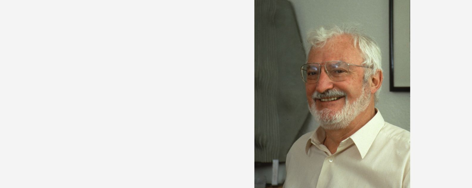
Heinrich Rohrer
The co-inventor of the scanning tunneling microscope won the Nobel Prize in Physics
The path to a Nobel Prize in Physics for Heinrich Rohrer began, quite unassumingly, on a house-hunting expedition. As a researcher at IBM’s Zurich Research Laboratory, he hired a young scientist from Germany named Gerd Binnig, who shared Rohrer’s fascination with atomic surfaces.
While looking for future residences, the duo exchanged frustrations over the fact that no scientific instrument existed to meaningfully explore the surface of an object at the atomic level. They decided to build their own. The scanning tunneling microscope (STM) would open an entire world to scientific study for the first time, hasten progress in the semiconductor industry and give rise to the field of nanotechnology.
Rohrer was born in Buchs, Switzerland, in 1933, half an hour after his twin sister. His family moved to Zurich in 1949, and a few years later Rohrer attended the Swiss Federal Institute of Technology (ETH). He received a bachelor of science degree in 1955 and a doctorate in experimental physics five years later — despite an interruption to serve in the Swiss Mountain Infantry.
Rohrer wrote his PhD thesis on superconductivity. The mechanical transducers used in some experiments were so sensitive, he later recalled, that he had to perform his tests after the busy town was asleep, often past midnight, to avoid vibration. This experience would prove critical to the development of the STM years later.
Getting to the essence of materials
Rohrer pursued a postdoctoral research fellowship at Rutgers University in New Jersey, where he concentrated on superconductors and metals, and joined IBM Research in 1963, the same year IBM opened its new research campus in Rüschlikon, Switzerland. By the late 1970s, he was intent on getting to the essence of surface materials, a critical area amid the rapid growth of the computer industry, particularly as semiconductor design was approaching the nanoscale.
In 1978, Rohrer insisted that IBM hire Binnig, a promising young physicist from Frankfurt University. The two men quickly sowed the seeds for the development of the STM to help visualize and even manipulate individual molecules and atoms.
A common optical microscope amplifies visible light through its lens. The STM works much differently. It uses the tiny electron-emitting tip of a tungsten needle, only a single atom wide, to slowly scan the surface of a sample from just a few angstroms above. A low electrical charge tunnels between the tip and the surface, and the current varies in strength depending upon the sample’s shape. These variations are measured and translated into a visual representation that resembles a three-dimensional topographic profile, which enables researchers to study the surface of a structure atom by atom.
The STM and similar scanning probe microscopes opened the door to the nanoworld and earned Rohrer and Binnig half of the Nobel Prize in Physics in 1986. German physicist Ernst Ruska received the other half of the prize for achievements in electron optics.
A natural leader
Rohrer spent his entire 34-year career at IBM, and in 1996 was named an IBM Fellow, the company’s highest technical distinction. He continued to focus on nanoscience, a field made possible by the invention of the STM. In 2011, IBM opened the Binnig and Rohrer Nanotechnology Center, a collaborative research facility in Rüschlikon, Switzerland.
Rohrer was an inspiration for many and was noted for being a sharp, witty and personable technological champion within IBM and the worldwide research community. While the Nobel was his crowning achievement, he went on to promote nanoscience and nanotechnology to generations of researchers. During one lecture in front of 4,000 South Korean high school and university students, he recalled the captivating journey to develop the STM and drew thunderous applause. “He was a natural leader, a visionary, a stimulating scientist and a wonderful person,” said Christoph Gerber, who collaborated with Rohrer at IBM for many years.
In an interview with the Nobel Foundation in 2008, Rohrer reflected on a life fueled by discovery. There were no tricks or shortcuts to breakthroughs, he said. His success was the product of insatiable curiosity, persistence and thinking differently. IBM granted him the freedom to make mistakes. "This freedom for scientists gets more and more lost. Otherwise, you do the common things. You don’t dare to do something beyond what everybody else thinks."
Rohrer credits this experimental approach to research as the key to developing the STM. “Binnig and I were not the types who would hang ourselves because of a failure,” he said.
Right up until he died in 2013, Rohrer remained hopeful for the future. He made a habit of mentoring the junior scientists at IBM Research and stoking the creative thinking and enthusiasm for research at the atomic level. “I am very pleasantly surprised with the young people,” he said. About the future, he added, “I think it’s in good hands.”
Related stories
The groundbreaking tool for viewing atomic-level behavior gave rise to nanotechnology
The co-creator of the scanning tunneling microscope opened the door to nanoscience and won a Nobel Prize
IBM pioneered exploration of the nanoscale, leading to breakthroughs from computing and biotech to climate science and AI