Product Documentation
Abstract
System board diagrams for the IBM xSeries 350
Content
Note: The illustrations in this document might differ slightly from your hardware.
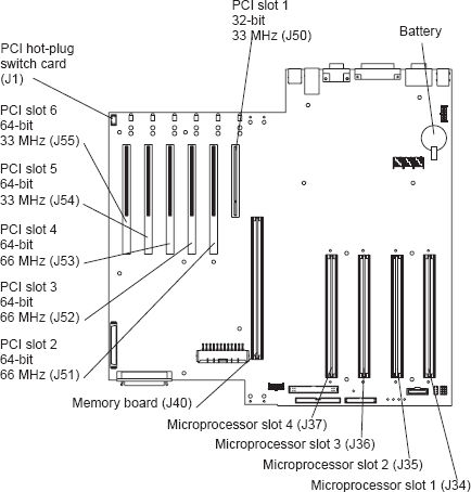
The following illustration shows the location of connectors on the system board:
| Back to top |
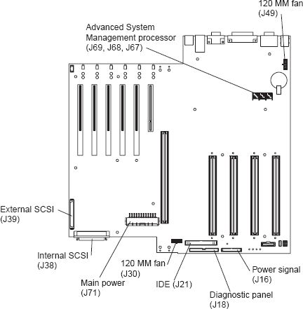
The following illustration shows the location of the cable connectors on the system board:
| Back to top |
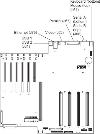
The following illustration shows the location of the input/output external port connectors on the system board:
| Back to top |
The following illustration shows the location of the flash ROM page swap jumper (J14) and power-on password overrid jumper (J15) on the system board:
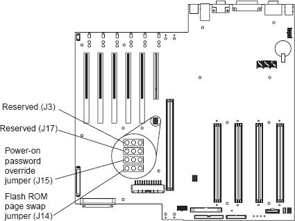
Notes:
- Turn off the server; then, disconnect all power cords and external cables before moving any jumpers.
- Jumpers J19 and J3 are located on the same jumper block as jumpers J14 and J15 on the system board. These jumpers are set to Disabled. Do not change the settings on these jumpers.
Attention: If you change the settings on these jumpers, the server will fail.
Jumpers J14 and J15 on the system board:
| Jumper name | Description |
|---|---|
| J14 Flash ROM page swap | The default position is a jumper installed on pins 2 and 3. |
| J15 Power-on password override | Changing the position of this jumper bypasses the power-on password check if the jumper has been moved since the server was last powered on. You do not need to move the jumper back to the default position after the password is overridden. The default position is a jumper on pins 2 and 3. Changing the position of this jumper does not affect the administrator password check if an administrator password is set. |
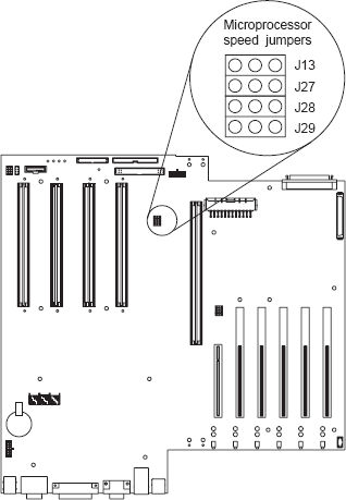
Jumper setback table:
| J13 | J27 | J28 | J29 | Bus Ratio | Core Frequency |
|---|---|---|---|---|---|
| H | L | L | H | 7:1 | 700 |
| H | L | H | L | 8:1 | 800 |
The following illustration shows the location of the microprocessor speed (core-frequency-selection) jumper block on the system board:
Note: Any system-board jumper blocks that are not shown in the illustrations in this book are reserved.
| Back to top |
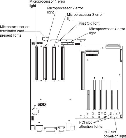
The following illustration identifies shows the location of the lights on the system board:
| Back to top |
The following illustration shows the location of the LEDs on the diagnostic panel. The diagnostic panel LEDs are visible through a special cutout area located to the left of the cover-release latch on the top cover. However, to determine the exact location of the error condition in the server, you might need to remove the top cover to view the location of the error LED on the diagnostic panel.
Note: The diagnostic panel is also called the LED card.
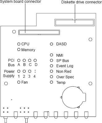
| The meanings of these LEDs are as follows | |
|---|---|
| CPU | Microprocessor fault |
| Memory | Memory fault |
| PCI Bus A (PCIA) | PCI bus A fault |
| PCI Bus B (PCIB) | PCI bus B fault |
| PCI Bus C (PCIC) | PCI bus C fault |
| PCI Bus D (PCID) | Not implemented at this time |
| Power supply 1 | Power supply numer 1 failure |
| Power supply 2 | Power supply numer 2 failure |
| Power supply 3 | Power supply numer 3 failure |
| FAN | Fan failure |
| DASD | Hard disk drive fault |
| NMI | Nonmaskable interrupt |
| SP Bus | Service processor failure |
| Event Log | Not implemented at this time |
| NON RED | Nonredundant power mode |
| OVER SPEC | Over specification |
| TEMP | System temperature failure |
Notes:
- The server does not support replaceable voltage regulator modules (VRMs).
- The server supports a maximum of three PCI buses.
- The server supports a maximum of three power supplies.
| Back to top |
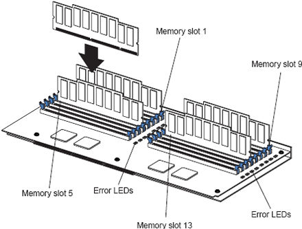
The following illustration shows the location of the dual inline memory module (DIMM) connectors and error LEDs on the memory board:
Notes:
- The illustrations in this document might differ slightly from your hardware.
- Some of the DIMM error LEDs are not visible in this illustration. The memory board contains 16 error LEDs; that is, one error LED for each DIMM connector.
| Back to top |
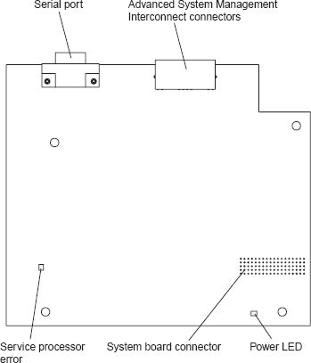
The following illustration shows the connectors and lights for the Advanced System Management Interconnect board:
Notes:
- The illustrations in this document might differ slightly from your hardware.
- The Advanced System Management Interconnect board is also called the service processor card.
| Back to top |
| Hardware Maintenance Manual - IBM eServer xSeries 350 |
Document Location
Worldwide
Was this topic helpful?
Document Information
Modified date:
24 January 2019
UID
ibm1MIGR-5070932