IBM Research
5 nanometer transistors inching their way into chips
June 5, 2017 | Written by: Huiming Bu
Categorized: IBM Research | Innovation
Share this post:
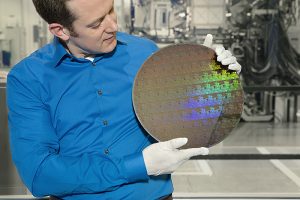
IBM Research scientist Nicolas Loubet holds a wafer of chips with 5nm silicon nanosheet transistors manufactured using an industry-first process that can deliver 40 percent performance enhancement at fixed power, or 75 percent power savings at matched performance. Press release link (Photo Credit: Connie Zhou)
Announced at the 2017 Symposia on VLSI Technology and Circuits conference in Kyoto this week, IBM and our research alliance partners, GLOBALFOUNDRIES and Samsung built a new type of transistor for chips at the 5 nanometer (nm) node.
To achieve this feat, the architecture – how the elements of a chip are arranged and the materials used – had to change.
We stacked layers of silicon nanosheets together, horizontally, in order for this new architecture to enable our 5nm transistor to deliver the power and performance boost future applications will demand. The change from today’s vertical architecture to horizontal layers of silicon opened a fourth “gate” on the transistor that enabled electrical signals to pass through and between other transistors on a chip. At these dimensions, it means that those signals are passing through a switch that’s no larger than the width of two to three DNA strands, side-by-side.
More ways to send a signal on more 5nm transistors equates to a 40 percent performance improvement over 10nm chips, using the same amount of power; or a 75 percent power savings, at the same performance level. (Let that sink in while reading this article on a mobile device with 10 percent power left: 5nm chips would give you hours, not minutes, before needing to recharge. A future 5nm-chip-powered mobile device will last days longer than what’s in your hand right now.)
Opening the path to more gates
Today’s chips with vertical “fin” transistors, called FinFET, power today’s most-powerful 14nm and 10nm chips, and even our own 7nm test chip announced two years ago. That third dimension of a fin allows for three gates for improved power and efficiency (versus, as you may have guessed, the previous generation’s 2D “planar” chips). These FinFET chips, only recently beginning to make their way into servers, computers, and devices, will be the standard for years to come. For reference, it takes 10 to 15 years of research and development before a groundbreaking new chip technology proliferates the market.
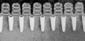
Pictured: a scan of IBM Research Alliance’s 5nm transistor, built using an industry-first process to stack silicon nanosheets as the device structure – achieving a scale of 30 billion switches on a fingernail-sized chip that will deliver significant power and performance enhancements over today’s state-of-the-art 10nm chips. (Photo credit: IBM)
The industry has long understood the limits of the various chip architectures. Our alliance working at the SUNY Polytechnic Institute Colleges of Nanoscale Science and Engineering’s NanoTech Complex in Albany, NY has known that, for example, it’s possible to build a 5nm FinFET transistor from a structural perspective. But scaling from our 7nm chip’s 20 billion FinFET transistors per chip, to 30 billion 5nm FinFET transistors would not deliver the significant power and performance boost mentioned above.
After about a decade of studying the idea of putting gates all around the transistor – often referred to as Gate-All-Around (GAA) – stacked nanosheets delivered a GAA transistor for the 5nm node that actually improved density, performance, and power – all built with industry manufacturable tools and processes.
Wait! What about Moore’s Law?
The mere introduction of new chip technology means this question comes up. Today, Moore’s Law, in the context of logic technology scaling, breaks down into four parts: density, performance, power and economy. Density, or the number of transistors per square inch of a chip, has gone from Gordon Moore’s original observation in 1965 of doubling every 12 months, to now taking three years. Performance improvements have experienced a similar slowing. Power, while less influential at its introduction, has grown in importance due to our battery-hungry mobile devices. The economy, or cost per transistor, is the only element of the “law” that’s kept similar pace over the last 50 years.
A future 5nm node chip with nanosheet transistors, and its scaled density, will deliver the expected value of performance, power, and economy.
At IBM, we think years ahead about what cognitive computing, cloud computing, blockchain, mobile, and security advances should be able to do – and what will make running those algorithms, and apps possible. We believe that billions of 5nm nanosheet transistors will soon serve as the silicon engine for these capabilities.

Director of Silicon Integration and Device Research, IBM Research

AI in 2020: From Experimentation to Adoption
AI has captured the imagination and attention of people globally. But in the business world, the rate of adoption of artificial intelligence has lagged behind the level of interest through 2019. Even though we hear that most business leaders believe AI provides a competitive advantage, up until recently, some industry watchers have pegged enterprise adoption […]

On Another Apollo Anniversary, a Reminder: IBM Space Technology Continues to Evolve
History’s publicists have done well by Apollo 11 and Neil Armstrong’s first moon steps in July 1969. However, fewer recall the Apollo 12 lunar mission four months later. It almost didn’t happen. On Nov. 14, 1969, in the first minute after lift-off, two lightning bolts struck Apollo 12. The spacecraft’s main power supply went dark, […]

The Apollo 11 Lessons We Live by Today
In 1969, more than 4,000 IBMers worked alongside NASA to land Apollo 11 on the moon. And for each day of the many months they worked writing code, programming computers and running simulations, they never stopped thinking: What else could we do? What contingency can we plan for? What are we forgetting? In fact, it […]